

In short
- A diode beam has two axes. An edge emitter leaves its narrow facet with a fast axis of typically 25–40° FWHM and a slow axis of 6–12°. The far field is elliptical, and the two axes usually have different beam quality and different waist positions.
- Measure the far field, not the facet. The far field starts about ten Rayleigh ranges from the emitter; for a broad-area emitter that is several millimetres, for a single-mode emitter a fraction of a millimetre.
- Take divergence from two planes. The emitter sits at an unknown depth inside the package. The difference between the widths at two sensor distances gives the angle without knowing where the emitter is.
- Wide beams need a Fourier lens or a screen. When the fast axis does not fit on the sensor in the far field, a lens maps angle to position (x = f tan θ), or a diffuse screen is imaged by the camera. The planner below picks the method.
What makes a laser diode beam different
Most lasers deliver a beam that is already collimated and close to round. A bare laser diode does not. Light leaves the edge of the chip through an emitting area that is about 1 µm high and anywhere from 2 µm (single-mode ridge) to 100–200 µm wide (broad-area and multi-junction pulsed emitters). Diffraction from that small, asymmetric aperture sets the beam.
The fast axis is perpendicular to the junction. The emitting height is close to the wavelength, so the beam spreads quickly, typically 25–40° full width at half maximum (FWHM), and it is close to diffraction-limited. The slow axis is parallel to the junction. The wider aperture gives a smaller angle, typically 6–12° FWHM, but in a broad-area emitter many lateral modes run at once, so its beam quality factor M² can be 10 to 50 or more. The far field is therefore an ellipse with an aspect ratio of about 3 : 1 to 5 : 1, and the two axes behave like two different lasers.
Datasheets give the divergence as a FWHM full angle. A camera-based laser beam profiler reports second-moment (D4σ) widths according to ISO 11146, and 1/e² widths. For a Gaussian profile the conversion is fixed:
θ1/e² = θFWHM × 2 ÷ √(2 ln 2) ≈ 1.70 × θFWHM
A 30° FWHM fast axis is about 51° at 1/e². The fast axis is close to Gaussian, so the conversion holds there. The slow axis of a broad-area emitter is often flat-topped or lobed, and its D4σ, 1/e² and FWHM angles can differ by tens of percent; state which one you use. The beam width definitions guide shows why.
Near field, far field and where to put the sensor
Near the facet the beam has the shape of the emitting area (the near field). Far from it the beam has the shape of its angular spectrum (the far field), and its width grows in proportion to the distance. Divergence is defined in the far field, so that is where it has to be measured.
A practical boundary is ten Rayleigh ranges. For a beam with 1/e² half-width w₀ at the waist and 1/e² half-angle θ, the Rayleigh range is zR = w₀ ÷ θ, and at z = 10 zR the width is within 0.5% of the straight-line far-field value. The fast axis reaches its far field within a few micrometres. The slow axis decides: a 100 µm broad-area emitter with an 8° FWHM slow axis has zR ≈ 0.42 mm, so its far field starts at about 4.2 mm. A 3 µm single-mode emitter is in the far field after about 0.13 mm.
The difficulty is that the fast axis has already grown large by then. At 5 mm, a 30° FWHM fast axis is about 4.8 mm wide at 1/e², and the ISO 11146 analysis area of three beam widths needs about three times that on the sensor. Whether the beam can be measured directly therefore depends on the size of the sensor, and on how close the package and the mechanics let you bring it.
The sensor faces the diode at two distances in the far field. Works when the fast axis still fits on the sensor there: large sensors, moderate divergence, single-mode VCSELs.
A lens with the emitter in its front focal plane and the sensor in its back focal plane maps each angle θ to the position f tan θ. Compact, independent of the emitter size, and the natural choice for VCSEL arrays.
The beam lights a flat diffuse screen; the camera images the screen. Any divergence and any beam size, at the cost of a geometric and cos³θ correction and a lower dynamic range.
Once the diode has its collimating optics, the beam is a few millimetres wide and is profiled like any other laser: widths, ellipticity, pointing and a caustic for M² in each axis.
Laser diode far-field planner
Enter the divergence from the datasheet, the slow-axis emitter width and the camera. The planner converts the angles to 1/e², finds where the far field starts and chooses between a direct measurement, a Fourier lens and a screen.
Camera details and mechanics
Model: Gaussian conversion θ1/e² = 1.70 θFWHM in both axes; slow-axis waist half-width = half the emitter width; zR = w₀ ÷ tan θ; far field from 10 zR; slow-axis M² ≈ π w₀ tan θ ÷ λ (an estimate from the datasheet values). The fast-axis 1/e² width must stay within ⅓ of the sensor width, leaving room for the ISO 11146 analysis area, and the slow axis needs at least 10 pixels. Direct: sensor between max(10 zR, closest distance) and the distance where the fast axis reaches ⅓ of the sensor. Fourier lens: f ≤ (W ÷ 3) ÷ (2 tan θfast), practical when f ≥ 3 mm and the NA needed to pass 1.5× the 1/e² half-angle, sin(1.5 θ), is 0.7 or less. Screen: at max(10 zR, 20 mm), screen width 3× the fast-axis 1/e² width. Multimode slow axes and VCSELs with rings are not Gaussian; use the result as a starting point.
Divergence from two planes, not one
A single far-field image gives a width D at a distance z, and the divergence would be about D ÷ z. The problem is z. The emitter sits behind a window, inside a TO can or a butterfly package, at a depth the datasheet gives only roughly, and the sensor surface lies behind its own cover glass. At a distance of 5 mm, an error of 0.2 mm in z is a 4% error in the angle.
The way around it is to measure the 1/e² or D4σ width at two distances z₁ and z₂, moved by a calibrated stage, and use only the difference:
θ = 2 atan[(D₂ − D₁) ÷ 2 (z₂ − z₁)]
The offset of the emitter cancels, and the stage reading is usually far more accurate than any estimate of where the chip is. Both planes must be in the far field, and the larger the step, the smaller the error: with a 3 mm step, a 10 µm stage error is 0.3% of the step. Extending the two planes to a series of ten, half near and half far as ISO 11146 describes, also gives the waist position and M² of each axis.
Two practical details. Align the camera so that its rows follow the junction plane, or read the orientation of the ellipse and take the widths along its axes; widths taken along tilted axes mix the fast and slow divergence. And keep the peak at 70–90% of full scale in both planes: the beam is several times brighter in the near plane, so the exposure or the attenuation changes between them, with a new background frame at each setting.
The Fourier lens and the screen
When the fast axis is too wide for the sensor at the first far-field distance, optics can bring the far field closer. A positive lens with the emitter in its front focal plane forms the far field in its back focal plane, at a distance of only 2 f. Every ray leaving the emitter at angle θ arrives at x = f tan θ, whatever its starting point on the emitter, so the image is the angular distribution itself. The divergence follows from the measured width as θ = 2 atan(D ÷ 2f).
- The NA must be large. The lens has to pass the beam out beyond its 1/e² angle: for a 30° FWHM fast axis that is an NA of about 0.6. Short-focus aspheric lenses designed for diodes reach it; ordinary lenses clip the wings and make the fast axis look narrower than it is.
- The angle scale must be calibrated. The nominal focal length and the lens distortion at large angles both scale the result. Tilt the diode, or a collimated reference beam, by a known angle and measure the centroid shift on the sensor; that gives millimetres per degree directly.
- The field must cover the emitter. For a single emitter this is trivial. For a VCSEL array or a diode bar the whole emitting area sits in the front focal plane, and the lens must image all of it to the same far field without vignetting.
A diffuse screen works for any angle. The beam lights a flat, uniform reflector at a distance L in the far field, and the camera, with its own lens, images the screen. Two corrections are needed: position on a flat screen grows as L tan θ, not L θ, and the irradiance falls as cos³θ away from the axis, because the path gets longer and the light arrives at a slant. At the 1/e² angle of a 30° FWHM diode the screen reads about 26% low unless this is corrected. Screens also lose dynamic range to speckle and scattered light, so they suit wide arrays and quick checks better than precise single-emitter work.
Astigmatism and the collimated module
In many diodes the fast and slow axes do not appear to come from the same point: the slow-axis waist lies a little behind the facet. This is astigmatism, and it is larger in gain-guided emitters than in index-guided ones. It is small at the chip, but optics magnify it: a lens system with transverse magnification m multiplies distances along the axis by m². A collimator and a focusing lens that image the emitter at ×20 turn a 5 µm astigmatic distance into 2 mm between the two foci.
Once the diode is collimated, it is profiled like any laser, and astigmatism shows up directly. Scan through the focus of a test lens and fit the width of each axis separately: the waists appear at different positions, the waist diameters differ, and so do the M² values. ISO 11146-1 covers this case, called simple astigmatism, when the principal axes of the ellipse stay fixed. If the ellipse rotates along the caustic (general astigmatism, for example after a misaligned cylindrical lens) the method of ISO 11146-2 is needed. The procedure and the fit are in the M² measurement guide, and for the small spots at the focus of a diode module see how to measure a focused laser spot size.
The same set-up checks the things a module datasheet promises: the ellipticity of the collimated beam, the residual divergence of each axis, and the pointing of the beam against the mechanical axis of the housing. For pointing over time and temperature, see laser pointing stability measurement.
VCSELs: round, but not always Gaussian
A vertical-cavity surface-emitting laser emits from the top of the chip through a round aperture of a few micrometres, so its beam is circular. A single-mode VCSEL has a Gaussian far field, with a full 1/e² angle of up to about 20°, and is the easiest case: a direct far-field measurement at two distances usually works.
Multimode VCSELs are different. Higher-order transverse modes put more power at the edge of the aperture, and the far field becomes a ring or a flat disc that changes with drive current and temperature. A 1/e² clip width of a ring describes its outer edge only, while D4σ includes the whole distribution. Specify which one the application needs, and record the profile at the operating current, not at threshold.
VCSEL arrays for sensing and illumination combine hundreds of emitters. Their far field is the sum of all emitters and often a shaped field from a diffuser; the Fourier lens is the natural method, with the whole array in its front focal plane. The near field, the uniformity from emitter to emitter, needs a magnified image of the chip. Many of these sources are pulsed, at 850, 905 or 940 nm, with pulses of a few nanoseconds; a global-shutter camera triggered by the driver captures them, as described in pulsed laser beam profiling.
What goes wrong, and how to see it
| Problem | What you see | What helps |
|---|---|---|
| Not yet in the far field | Slow-axis divergence too small; it grows when you move the sensor back | Measure beyond 10 slow-axis Rayleigh ranges |
| One-plane distance error | Divergence off by a few percent, different on every set-up | Two planes on a calibrated stage, θ from the width difference |
| Fast axis clipped | Fast-axis angle too small, profile cut flat at the sensor edge or lens rim | A larger sensor, a Fourier lens with enough NA, or a screen |
| Camera axes tilted to the junction | Ellipticity too low, fast and slow angles closer than the datasheet | Rotate the camera, or take the widths along the measured ellipse axes |
| Saturation in the near plane | Flat-topped profile at the closest distance, width too large | Peak at 70–90% of full scale in each plane, background frame per setting |
| Back-reflection into the diode | Power or profile flickers, mode hops, noise | Tilt the sensor or filter by a few degrees; an isolator for sensitive single-mode diodes |
| Wrong drive conditions | Slow axis wider or narrower than expected | Measure at the operating current and temperature; the slow axis changes with both |
How to specify a diode beam
A diode divergence number is only comparable when its conditions are stated. A complete record gives:
- Angle and definitionFWHM, 1/e² or second-moment (D4σ), full or half angle, for each axis
- Axesfast and slow, aligned to the junction or the principal axes of the ellipse
- Methoddirect two-plane, Fourier lens with its focal length and calibration, or screen
- Operating pointdrive current, pulse width and repetition rate, case temperature
- For modulescollimated beam size, ellipticity, M² and waist position per axis, pointing
For a diode or module in production, these values become pass/fail limits with guard bands; the method is in laser beam profiler production QA.
IZAK products for this application
IZAK laser beam profilers are camera-based, with second-moment widths according to ISO 11146, and report the ellipticity and orientation of elliptical beams. We configure the sensor, a Fourier lens or relay optics and the attenuation for your diode, VCSEL or module.
 Beam profiling · 300–1100 nmUV–VIS–NIR Laser Beam ProfilersFor visible and near-infrared diodes and VCSELs, including large-sensor models for direct far-field measurements.View product →
 Beam profiling · up to 2.05 µmSWIR Laser Beam ProfilersFor telecom and eye-safe diodes at 1310 and 1550 nm and other short-wave infrared sources.View product →
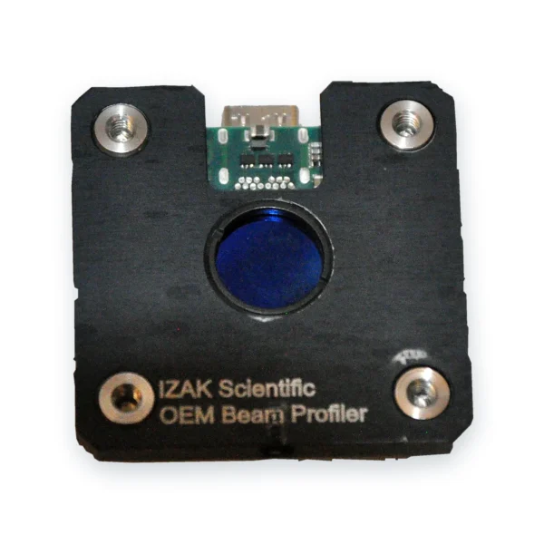 OEM · board levelOEM Board-Level Laser Beam ProfilersCompact global-shutter profilers for diode and module test stations in production.View product →
Longer wavelengths: MWIR 1.5–5.7 µm and LWIR 7.7–12 µm for mid-infrared and long-wave semiconductor lasers. Still choosing? Read how to choose a laser beam profiler or the complete guide to laser beam profiling.
What to send us for a recommendation
With these details an engineer can propose the camera, the optics and the attenuation for your diode:
- Source type and wavelengthedge emitter, VCSEL, array or collimated module
- Datasheet divergencefast and slow axis, and how it is defined
- Emitter or array sizeand the package: TO can, butterfly, chip on submount
- CW or pulsedpulse width, repetition rate, peak and average power
- What you need to verifydivergence, ellipticity, M², astigmatism, near-field uniformity
- Where it will be usedlab, incoming inspection or a production test station
Frequently asked questions
QHow do you measure the beam profile of a laser diode?
QWhat are the fast axis and the slow axis of a laser diode?
QHow do I convert FWHM divergence to 1/e²?
QWhere does the far field of a laser diode start?
QWhy measure divergence at two distances?
QHow is a VCSEL beam profiled?
References
- ISO 11146-1: Lasers and laser-related equipment — Test methods for laser beam widths, divergence angles and beam propagation ratios — Part 1: Stigmatic and simple astigmatic beams.
- ISO 11146-2: Lasers and laser-related equipment — Test methods for laser beam widths, divergence angles and beam propagation ratios — Part 2: General astigmatic beams.
- ISO 11146-3: Lasers and laser-related equipment — Test methods for laser beam widths, divergence angles and beam propagation ratios — Part 3: Intrinsic and geometrical laser beam classification, propagation and details of test methods.
- ISO 13694: Optics and optical instruments — Lasers and laser-related equipment — Test methods for laser beam power (energy) density distribution.
Tzachi Sabati
CEO, IZAK Scientific
Physicist specializing in photonics and quantum technologies, with deep expertise in quantum sensors and advanced optical systems. Leads the Advanced Quantum Lab course at the Technion, bridging academic excellence with industry innovation. At IZAK Scientific, provides cutting-edge photonics-based solutions, developing customized inspection and sensing systems for R&D and production. Passionate about advancing quantum sensing applications and integrating novel technologies to meet industry needs.
Get new IZAK guides and tools by email
One short email a month: new technical articles, free calculators and product updates in laser measurement and electro-optics. No spam, unsubscribe anytime.
