

In short
- Electro-optics covers the whole spectrum. Projects run from UV through visible and NIR to SWIR, MWIR and LWIR: light sources, optical models and upgrades of existing systems.
- Six elements make a good design process: field of view and depth of field, uniformity and divergence, responsivity and noise, the application’s own requirements, a test and measurement plan, and documentation to ISO 9001:2015.
- Size the optics early. Use the calculator below to check field of view, depth of field and resolution on the object before you order a lens.
- Complex projects need experts. An experienced optical design team reuses proven architectures instead of starting from scratch.

Optical engineering is needed in many kinds of technology development: building light sources, creating optical models of a system, and improving projects that already exist. The work can cover the full optical spectrum, from ultraviolet (UV) through visible and near-infrared (NIR) to the short-wave, mid-wave and long-wave infrared bands (SWIR, MWIR and LWIR).
So what should a good electro-optical design process include? Below are the six elements we check in every project, a calculator for the first of them, and a short guide to when you should bring in an optical design team.
Six elements of a good electro-optical design process
Optimize the area the system sees and the range of distances over which it stays in focus. Focal length, detector size, working distance and f-number decide both, and they trade against light collection.
Check the uniformity of the illumination or the beam, and its divergence, and correct them where needed. Non-uniform light or an unexpected divergence shows up later as measurement error.
Optimize how strongly the detector responds to the light you actually deliver to it, and reduce noise from the detector, the electronics and stray light, so the signal stays well above the noise floor.
Adapt the design to the specific application: wavelength, power, speed, environment, size, cost and the way the system will be used and maintained.
Define the tests and the measurement systems early. Decide how each requirement will be verified, at which stage, and with which instrument and pass/fail limit.
Make sure all documentation meets the ISO 9001:2015 standard: requirements, design reviews, test reports and revisions, so the system can be built, verified and supported over its life.
The order matters less than the habit: each element is reviewed at the start of the project, revisited at every design review and closed with a measurement. For the electronics and real-time processing side of the same system, see The Best Use of FPGA in Your Electro-Optics Setup; for thermal control of detectors and lasers, see Thermoelectric Coolers and TEC Testing.
Field of view and depth of field calculator
Enter the detector width, pixel pitch, lens focal length, working distance and f-number. The tool returns the field of view on the object, the angular field, the size of one pixel on the object and the depth of field for the blur you accept.
Thin-lens model. Magnification m = f/(s − f); field of view = detector width / m; angular field = 2·atan(field / 2s). Hyperfocal distance H = f²/(N·c) + f; near limit = s(H − f)/(H + s − 2f); far limit = s(H − f)/(H − s), or infinity when s ≥ H. A blur circle of about two pixels is a common choice. Real lenses add aberrations and diffraction (blur ≈ 2.44·λ·N), so confirm the final design with a lens model and a measurement.
When to bring in optical design experts
Some projects need more complex planning, design and operation than an in-house team can cover. In those cases, hiring optical design experts saves time and risk:
- Experience from many projects. Experts have worked on many systems and bring that knowledge to the planning and design of yours.
- No need to start from scratch. A broad background in optical and electronic engineering means existing, proven architectures can be reused and adapted.
- Optimized light sources and detection. When you develop a light source, or a light source together with a toolbox of detectors and technologies, experts can optimize the whole chain from emitter to signal.
Read more on what to look for in Choosing an Electro-Optical Experts Team, and on verifying optical surfaces in Interferometer Testing for Precision Flatness Measurement. If your system includes a laser, the beam itself is part of the test plan: a laser beam profiler and the Gaussian beam calculator help you check beam size, divergence and uniformity.
IZAK products for this application
Instruments from our catalog that match the measurements and set-ups in this article.
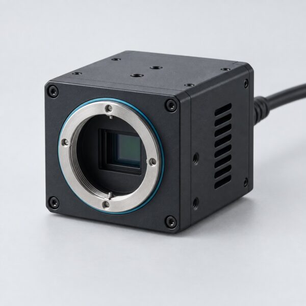 Laser metrologyLaser Beam ProfilersUV to LWIR families, packaged, OEM or software, with Test mode and reports.View product →
 Optical powerMulti-Channel Power MeterParallel optical power on several fiber-coupled channels, with logging software.View product →
 RadiometryMulti-Channel Spectro-RadiometerSpectral and radiometric measurement on several channels at once.View product →
Need something that is not in the catalog? We design custom electro-optical systems →
Frequently asked questions
QWhat are the main steps in designing an electro-optical system?
QHow do I calculate field of view and depth of field for an imaging system?
QWhen should I hire optical design experts?
Tzachi Sabati
CEO, IZAK Scientific
Physicist specializing in photonics and quantum technologies, with deep expertise in quantum sensors and advanced optical systems. Leads the Advanced Quantum Lab course at the Technion, bridging academic excellence with industry innovation. At IZAK Scientific, provides cutting-edge photonics-based solutions, developing customized inspection and sensing systems for R&D and production. Passionate about advancing quantum sensing applications and integrating novel technologies to meet industry needs.
