
Optical sensors play a critical role in radiometry and scientific instrumentation, converting incident radiant energy into measurable electrical signals. They span a wide range of operating principles – from quantum (photon-counting) detectors like semiconductor photodiodes and photomultipliers to thermal detectors like bolometers and pyroelectrics. This article provides an in-depth technical review of the full range of optical sensors, including traditional devices and emerging technologies. We discuss semiconductor photodiodes (Si, InGaAs, HgCdTe, etc.), photoconductive and photoemissive photon detectors (including photoconductors and photomultiplier tubes), thermal detectors (bolometers, pyroelectric sensors, thermopiles), and newer sensor concepts (e.g. nanowire-based sensors and single-electron/photon detectors). For each type, we outline the operating principle, spectral sensitivity, key performance metrics (detectivity D★, noise-equivalent power (NEP), responsivity, response time), physical characteristics (size, cooling, materials), and example applications. A comparative summary table is also included to contrast key specifications across sensor types.
Semiconductor Photodiodes (Photovoltaic Detectors)
Operating Principle: Semiconductor photodiodes are photovoltaic detectors that generate a photocurrent when photons are absorbed in a semiconductor p-n or p-i-n junction. Under reverse bias (photoconductive mode) or zero bias (photovoltaic mode), each absorbed photon creates electron-hole pairs, producing a current proportional to light intensity [4]. Photodiodes are highly linear and exhibit fast response and high quantum efficiency across broad spectral bands[4].
Spectral Sensitivity: The spectral response of photodiodes is governed by the semiconductor bandgap. Silicon (Si) photodiodes cover ~190 nm to 1100 nm (UV–visible–NIR), peaking near 800–900 nm with responsivities ~0.5–0.6 A/W. Germanium (Ge) and InGaAs photodiodes extend into the NIR: Ge covers ~800–1800 nm but with higher dark current, while InGaAs (Indium Gallium Arsenide) covers ~900–1700 nm (standard) and can be extended to ~2500 nm with modified alloys[4]. InGaAs photodiodes offer superior sensitivity in the 1–1.7 µm telecom band with lower dark noise than Ge. Extended InGaAs and InAsSb detectors can reach 2–5 µm (MWIR) but at the cost of much higher dark current, often requiring thermoelectric cooling [4]. Mercury Cadmium Telluride (HgCdTe or MCT) can be engineered for a wide IR range (1–25 µm) by tuning its bandgap via composition[3]. MCT photodiodes (often cooled to 77 K) cover mid-IR to long-wave IR; they can be optimized for specific wavelengths (e.g. 5 µm, 10.6 µm CO₂ laser line) by adjusting the Hg/Cd ratio[3].
Key Performance Metrics: Photodiodes typically achieve very high detectivity. Silicon photodiodes, for example, exhibit D★ on the order of 10^12–10^14 Jones (cm·Hz^½/W) in the visible range[1], thanks to low noise and high responsivity. Advanced Si devices with internal gain have even demonstrated D★ ~10^14 Jones at 940 nm[5]. InGaAs photodiodes also reach D★ ~10^12–10^13 Jones in the NIR, significantly outperforming legacy Ge detectors (Ge D★ ~10^11 or lower, due to higher dark current)[4]. MCT photodiodes (cooled) achieve D★ in the 10^10–10^11 range at mid-IR wavelengths[2] – roughly 10–50× higher sensitivity than room-temperature pyroelectric sensors[2]. Noise-equivalent power (NEP) for small-area Si or InGaAs photodiodes can be as low as 10^−15 to 10^−14 W/√Hz. Photodiode responsivity varies with wavelength (e.g. Si ~0.2 A/W at 400 nm rising to ~0.6 A/W at 900 nm), and quantum efficiency can exceed 80–90% near peak wavelengths. Response times are fast, on the order of nanoseconds to microseconds, limited by junction capacitance and transit time. For example, Si PIN photodiodes can have <1 ns rise times, supporting GHz bandwidth, while large-area InGaAs detectors (with higher capacitance) have slower response in the tens of MHz range. Avalanche photodiodes (APDs) introduce internal gain by operating the diode near breakdown. Si APDs (for 400–1000 nm) and InGaAs APDs (1000–1700 nm) can detect low light with gain M10–100, but at the cost of added noise (excess noise factor ~2–5). Still, APDs improve the SNR in photon-starved applications and achieve timing jitter in the tens of picoseconds, useful for LIDAR and time-correlated single photon counting. Modern Si APDs or single-photon avalanche diodes (SPADs, operated in Geiger mode) can resolve single photons with photon detection efficiencies ~50% at 500 nm, though requiring careful quenching circuits and having dark count rates on the order of a few Hz to kHz depending on cooling.
Physical/Electrical Characteristics: Photodiodes are compact solid-state devices (millimeter-scale or smaller active areas). They typically operate at room temperature (except narrow-bandgap types like extended InGaAs or MCT, which often use thermoelectric or cryogenic cooling to suppress dark current). Cooling a photodiode reduces thermal noise and can dramatically increase D★ for IR diodes[2]. Photodiodes are typically packaged in hermetic enclosures with optical windows (e.g. quartz for UV/vis, silicon for NIR, or ZnSe for mid-IR). Some IR photodiodes use immersion microlenses to boost effective area and detectivity by concentrating light[4]. Reverse bias is applied in photoconductive mode to improve speed at the cost of higher dark current[4].
Example Applications: Owing to their accuracy and speed, semiconductor photodiodes are widely used in radiometric instruments and photometry. Silicon photodiodes serve as standard detectors for laser power meters, photometric sensors, and solar irradiance monitors (with NIST-traceable calibration). They are used in trap detectors for optical power standardization due to very predictable responsivity. InGaAs photodiodes are critical in fiber-optic communication receivers (1.3 and 1.55 µm) and in near-IR spectroscopy (e.g. optical coherence tomography, LIDAR). MCT photodiodes find use in thermal imaging, gas analysis (IR spectrometers/FTIR), and remote sensing; for example, cooled MCT detectors in Fourier-transform infrared (FTIR) spectrometers vastly outperform thermal DTGS pyroelectric detectors, offering ~100× higher sensitivity and MHz-frequency response for fast spectral scans[3]. Avalanche photodiodes and SPADs are used for single-photon counting in fluorescence lifetime measurements, quantum communication, and photon correlation studies, as well as in hazard detection (e.g. LIDAR laser ranging and atmospheric aerosol LiDAR).
Photon Detectors: Photoconductive and Photoemissive Sensors
Photon detectors in this category directly convert incident photons to an electrical signal via either a change in conductivity (photoconductive effect) or via photoelectric emission of electrons. Unlike photovoltaic diodes, these often require an external bias or vacuum tube for operation. They generally offer higher sensitivity (especially when cooled) but may require high bias voltages or cooling and can have slower response or more complex readout.
Photoconductive Detectors (Bulk Photoconductors): A photoconductor is typically a semiconductor material where incident photons excite carriers, increasing its electrical conductivity. A bias voltage applied across the material then produces a photogenerated current. Classic examples are the lead salt detectors: PbS (lead sulfide) and PbSe (lead selenide) photoconductors, historically used for mid-infrared (1–5 µm) detection. PbS/PbSe sensors are often operated at or slightly below room temperature (sometimes with Peltier cooling to ~–30 °C to reduce noise). Their spectral ranges cover roughly 1–3 µm for PbS and 1–5 µm for PbSe, with peak sensitivity around 2–3 µm. These detectors have modest detectivities – e.g. PbSe can achieve D★ on the order of 10^9 Jones at room temperature[2], which is an order of magnitude higher sensitivity than thermal pyroelectrics (~10^8) but far lower than cooled semiconductor photodiodes[2]. They also have slower response ( bandwidths ~ tens to hundreds of kHz ), limited by carrier trapping and recombination dynamics. Modern variants of photoconductors include extrinsic silicon detectors (doped Si detecting IR via impurity levels, requiring cryogenic cooling) and HgCdTe photoconductors. HgCdTe (MCT) photoconductive detectors operate by biasing a HgCdTe element; they were widely used in thermal IR cameras and spectrometers before HgCdTe photodiodes became common. MCT photoconductors offer very high responsiveness and could surpass pyroelectrics by factors of 10–100 in D* when cooled[12], but they exhibit 1/f noise and require precise temperature control. Another important class are quantum well infrared photodetectors (QWIPs), which are essentially photoconductive quantum devices: they use intersubband transitions in multiple quantum well structures (e.g. GaAs/AlGaAs) to absorb IR (typically 8–12 µm LWIR) and free carriers into a conduction band under bias. QWIPs require cryogenic cooling (~70 K) and have lower peak D* (~10^9–10^10) compared to HgCdTe, but offer excellent uniformity and large-format FPAs for thermal imaging[9]. Emerging photoconductors also include quantum dot infrared photodetectors (QDIPs) and perovskite or 2D material photoconductors, where nanostructures provide broadband absorption and potentially higher operating temperatures[9].
Performance: Photoconductors generally need bias and often exhibit higher noise (due to dark current and Johnson noise in the bias circuit) than photovoltaic diodes. Their NEP is improved by cooling to reduce thermal excitations. For instance, an InSb photoconductor (cutoff ~5.5 µm, cooled to 77 K) can reach D* ~2×10^11 Jones[2], whereas at 300 K it would be orders of magnitude lower. Response times range from microseconds (in thin-film or small devices) to milliseconds for large-area or slow-responding materials. Many photoconductors also require chopped or modulated measurements (with lock-in amplifiers) to mitigate 1/f noise and drift.
Photoemissive Detectors (Phototubes and PMTs): Photoemissive sensors operate via the external photoelectric effect: incident photons strike a photosensitive cathode material in vacuum, causing emission of electrons. These emitted photoelectrons are then collected or amplified. The simplest device is a vacuum photodiode (phototube), with a photocathode and an anode; more important are photomultiplier tubes (PMTs), which add a cascade of dynodes for electron multiplication. In a PMT, a single photon can liberate one electron from the cathode, which is then accelerated to a dynode, knocking out several secondary electrons, and so on through ~10 stages – yielding an enormous gain (~10^6 electrons per photon). This internal gain and low noise current make PMTs ultra-sensitive. They achieve effective NEP levels on the order of 10^−16 to 10^−18 W/√Hz, enabling single-photon detection in the UV–visible range[7]. Spectral range: Photocathodes are selected for the band of interest – common PMT photocathodes (bialkali, multialkali compounds like Sb–K–Cs) cover ~185 nm (deep UV) to ~900 nm. Specialty cathodes (e.g. GaAs or InGaAs) extend sensitivity into the near-IR (1.0–1.7 µm) at the cost of higher dark current. PMTs typically have peak quantum efficiencies around 20–30% (higher for newer GaAsP photocathodes in the blue).
Performance: Detectivity: Since PMTs are usually limited by shot noise of dark current or ambient background, their performance is often stated in terms of dark count rate and gain rather than D, but effectively their D* can be >10^14 Jones in photon-counting scenarios, far exceeding semiconductor diodes in the visible. They have fast rise times (sub-nanosecond pulses are achievable in fast PMTs), though large-area or longer path PMTs have transit time spreads of a few ns. PMTs require a high-voltage supply (typically 500–1500 V) for the dynodes. They are bulky (glass vacuum tubes) and can be fragile, and they can be damaged by exposure to intense light. Nevertheless, for extremely low light flux measurements, PMTs remain a gold standard due to their combination of gain and low noise[7].
Example Applications: Photoconductive detectors like PbS/PbSe were used in early IR spectrophotometers and are still found in some inexpensive gas sensors or handheld IR analyzers. MCT photoconductors and QWIPs have been used in thermal imaging cameras and astronomy (IR focal plane arrays). Photoemissive PMTs, on the other hand, are pervasive in scientific instrumentation: e.g. scintillation counters for radiation detection (where a scintillator converts high-energy radiation to visible photons detected by a PMT), fluorescence spectrometers, single-photon counting experiments, LIDAR receivers (e.g. atmospheric LIDARs for aerosols), and astronomy photon-counting detectors. A notable example is the use of PMTs in Cherenkov telescopes and neutrino observatories to capture faint light flashes. Microchannel plate (MCP) PMTs and image intensifiers are specialized photoemissive devices providing sub-nanosecond response and two-dimensional imaging (as in night-vision goggles or streak cameras). In recent years, solid-state analogs of PMTs such as the silicon photomultiplier (SiPM) – essentially an array of Geiger-mode APD microcells – have gained popularity. SiPMs operate at low bias (~30 V), are compact and insensitive to magnetic fields, and achieve single-photon sensitivity with gain ~10^6, making them viable replacements for PMTs in applications like medical PET scanners and portable radiation detectors. However, SiPMs have higher dark counts and smaller area than large PMTs, and they are currently used mainly for visible light detection.
Thermal Detectors (Bolometers, Pyroelectric Sensors, Thermopiles)
Thermal detectors rely on absorption of radiation as heat and a subsequent change in some temperature-dependent property (resistance, polarization, etc.). Unlike photon detectors, thermal sensors have a flat spectral response over a very broad range (from UV to far-IR and even terahertz), since any photon absorbed will heat the sensor. They are useful for broadband radiometry and where the wavelength range is too long for convenient semiconductor detectors (far IR, THz), but they generally have slower response and lower sensitivity (especially at fast time scales) compared to cooled photon detectors[3].
Bolometers: A bolometer consists of an absorber (which converts incident radiation to heat) thermally linked to a reservoir (heat sink). As the absorber heats up, its temperature rises relative to the heat sink. The temperature change is read out via a temperature-sensitive element. In a resistive bolometer, the element is often a thermistor material whose resistance drops or rises with temperature. Early bolometers used blackened metal strips (e.g. platinum) with resistance changing per incident power; modern microbolometers use MEMS-fabricated bridges of materials like vanadium oxide (VOx) or amorphous silicon, which have high temperature coefficient of resistance (TCR). Operating principle: The bolometer is biased in a readout circuit, and light-induced resistance change is measured. Bolometers do not require cooling (though cooling greatly improves sensitivity by reducing thermal noise). Spectral range: effectively 0.1–1000 µm (limited only by absorber coating and window transmission). Performance: Uncooled microbolometer pixels (operated at ~300 K) in thermal cameras typically achieve NETD (noise-equivalent temperature difference) ~50 mK, corresponding to NEP on the order of 10^−10 to 10^−9 W/√Hz per pixel and specific detectivity D★ ~10^8–10^9 Jones in the 8–14 µm band. This is lower than cooled photon detectors (MCT or InSb) by orders of magnitude[3], but microbolometers’ advantage is room-temperature operation and low cost in large arrays. Their response time is on the order of milliseconds (thermal time constant ~10–20 ms for typical 17 µm pixel bolometers[3]), sufficient for video frame rates (~30 Hz) but not for high-speed modulation. To improve sensitivity for scientific use, bolometers are often cooled. Cooled bolometers: For example, at liquid helium temperatures (4 K or even 0.1 K in advanced systems), bolometers can be extraordinarily sensitive, limited only by thermal fluctuation noise or even photon noise from the background. Cooled bolometers (using semiconductor thermistors or superconducting sensors) are used in far-infrared astronomy – e.g. the SPIRE instrument on the Herschel space telescope used an array of transition-edge sensor bolometers at 0.3 K to detect sub-millimeter radiation with NEPs ~10^−17 W/√Hz. Cooled bolometers can have D★ well above 10^12 in the far-IR where photon detectors are impractical[13]. However, cooled bolometer systems require complex cryogenics and slow readouts.
Pyroelectric Detectors: Pyroelectric sensors use crystalline materials that have a temperature-dependent spontaneous polarization (e.g. deuterated triglycine sulfate – DLaTGS, or lithium tantalate). When the temperature of the crystal changes, the change in polarization generates a displacement current that can be measured as a signal (usually via a JFET or op-amp). Pyroelectrics respond only to changes in incident radiation (they are AC-coupled detectors), so they typically require the incident radiation to be modulated (chopped) or the target to be moving. Spectral response: broadband (UV to far-IR) since a black coating on the crystal absorbs the radiation. Performance: Pyroelectric detectors operate at room temperature. DLaTGS (a deuterated TGS variant) is a common material in FTIR spectrometers. A typical DLaTGS pyroelectric might have D* ≈ 2×10^8 Jones at 10 µm with a 1 Hz chopping frequency[2]. This is substantially less sensitive than a cooled MCT photodiode (by a factor of ~200 in the example from Thermo Nicolet)[2], but pyros are still useful when simplicity and broad spectral coverage are needed. Pyroelectrics have moderate response times, often in the sub-millisecond range for thin elements (they can be faster than thermopiles or bolometers because the thermal mass is small). For example, pyroelectric video sensors exist (the classic “IR motion sensor” in alarms uses a pyroelectric that can respond in <0.1 s to movement). In FTIR, pyroelectric detectors can handle modulation frequencies up to a few kHz. To improve stability, modern pyroelectric detectors often include temperature stabilization or are operated in a temperature-controlled enclosure, since the output can drift with ambient temperature changes.
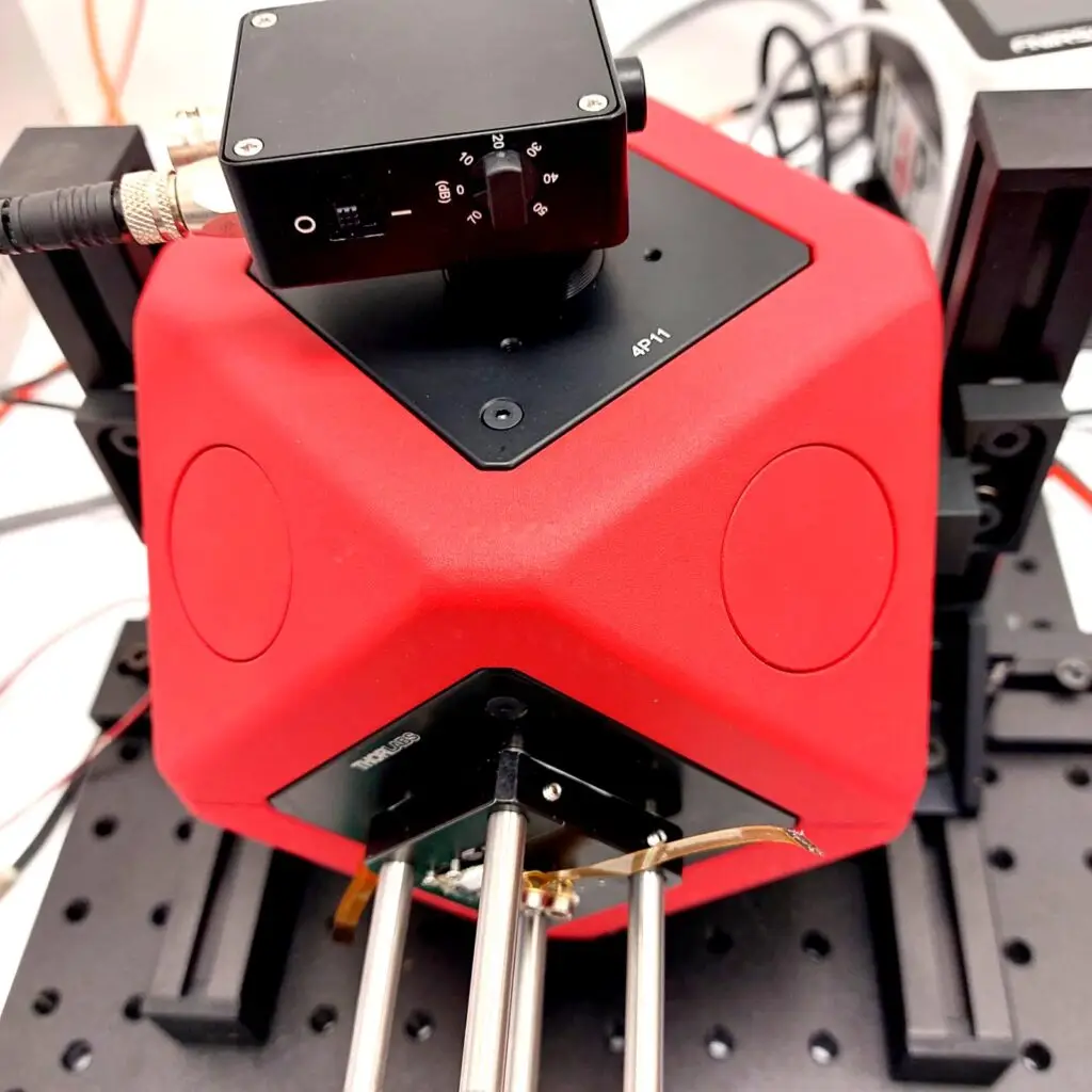
Cooled multi-channel spectro-radiometer by IZAK Scientific, featuring high-speed IR or VIS spectrometers with linear detector arrays—ideal for precise radiometric characterization. The system includes narrow FOV optics (tens of mrad), flat 5 MHz bandwidth (–3 dB), <10% non-uniformity, replaceable ND filters, and full software integration. Learn more: izakscientific.com/product/multi-channel-spectro-radiometer.
Thermopile Detectors: A thermopile is essentially a series of thermocouple junctions connected in series to amplify the voltage output. One set of junctions (the “hot” junctions) is on an absorbing thermal element, and the other set (the “cold” junctions) is on a reference at a lower temperature. When radiation is absorbed, the temperature difference generates a voltage via the Seebeck effect. Spectral range: very broad (a blackened thermopile can absorb from UV to far-IR). Performance: Thermopiles produce a DC output proportional to absolute incident power (unlike pyroelectrics, which need chopping). They are very stable and linear, but generally less sensitive and slower. D* for thermopiles is usually in the 10^7–10^8 range. For instance, a small thermopile (area ~2 mm^2) might have NEP ~10^−9 W/√Hz (D* ~10^8) and a response time of tens of milliseconds. The output voltages are on the order of a few tens of microvolts per µW, so low-noise amplifiers are required. Thermopiles are widely used in portable radiometers and heat flux sensors (e.g. pyranometers for measuring solar irradiance, where a thermopile measures broadband solar power). They are also common in non-contact IR thermometers and low-cost thermal arrays (like the MLX90640 32×24 thermopile array used for thermographic imaging without microbolometers).
Comparative Note: Among thermal detectors at room temperature, pyroelectric sensors often offer better sensitivity and faster response than thermopiles or bolometers[14]. In fact, LiTaO₃ pyroelectric arrays can achieve performance intermediate between cooled photon detectors and uncooled bolometers[14]. Bolometers (uncooled) typically have to trade off speed for sensitivity – e.g. increasing thermal isolation improves D* but slows the response. Pyroelectrics, being AC-coupled, are ideal in scenarios with modulated signals, whereas thermopiles are preferred for true DC measurements (e.g. measuring a steady thermal radiation level). All thermal detectors benefit from techniques like chopping or signal averaging to reach their noise floor.
Example Applications: Thermal detectors are indispensable for broadband and long-wavelength radiometry. Bolometers: Uncooled microbolometer arrays are the basis of most thermal infrared cameras for night vision, surveillance, and thermal diagnostics (wavelengths 7–14 µm). Large-format bolometer arrays (e.g. 640×480 pixels at 17 µm pitch) can produce high-resolution thermal images at video rates. In scientific use, sensitive cooled bolometers (often superconducting TES bolometers) are deployed in telescopes to detect cosmic microwave background or sub-mm cosmic signals. Pyroelectric detectors: Used in FTIR spectrometers (where the interferometer’s output is modulated by a chopper, a pyroelectric can measure the interferogram over a wide IR spectrum). They are also used in gas analyzers (NDIR sensors) and intruder motion sensors (the familiar PIR sensor that detects a person by the change in IR heat signature across multiple pyroelectric elements). Thermopiles: Common in handheld radiation thermometers (point-and-shoot IR thermometers measure thermal emission from objects), in laser power meters (for measuring high laser powers over broad wavelengths – a thermopile disk can absorb the beam and measure its heating), and in climate research instruments (e.g. pyrheliometers for direct solar beam measurement). Thermopile sensor modules (with integrated optics and amplifiers) are also used for CO₂ sensing by NDIR (detecting IR absorption dips), where the absolute stability of a thermopile is advantageous.
Emerging and Advanced Optical Sensors
The push for greater sensitivity, bandwidth, and new wavelength capabilities has led to novel sensor technologies. Some leverage nanostructured materials or quantum effects to detect extremely small optical signals – down to single photons or even single electrons – with high efficiency. Below we highlight a few emerging sensor types and concepts:
Superconducting Nanowire Single-Photon Detectors (SNSPDs): SNSPDs consist of a thin superconducting nanowire (often Niobium nitride or similar, only ~5–10 nm thick and ~100 nm wide) patterned into a meandering filament. The nanowire is biased with a current just below its superconducting critical current. When a single photon is absorbed, it locally breaks the superconductivity (creating a “hotspot”), forcing the current to divert and creating a momentary resistive voltage pulse. The wire then cools and returns to superconducting state, ready for the next photon. Performance: SNSPDs typically operate at cryogenic temperatures (2–4 K, often using liquid helium or closed-cycle cryocoolers). They achieve detection efficiencies of 70– Ninety% at specific wavelengths (e.g. telecom 1550 nm) with virtually zero dark counts when well shielded. Their timing jitter can be as low as ~20 ps, making them the fastest single-photon sensors available. NEP values for SNSPDs can reach the 10^−20 W/√Hz scale (implied by single-photon sensitivity and low dark count) – orders of magnitude better than any room-temp detector. They have broad sensitivity from visible to mid-IR (material dependent; NbN SNSPDs cover ~500–2000 nm, while other materials like WSi extend to ~10 µm in research). Applications: Because of their unparalleled photon-counting performance, SNSPDs are used in quantum optics (entangled photon detection, quantum key distribution receivers), single-photon LiDAR, fluorescence lifetime measurements at extremely low concentrations, and emerging astronomical instruments (e.g. for single-photon counting of faint time-variable stars or optical SETI). The downside is the need for cryogenic cooling and specialized readout (fast pulse counting electronics).
Transition-Edge Sensors (TES) and Microwave Kinetic Inductance Detectors (MKIDs): These are superconducting detectors designed to count or resolve single photons with energy measurement. A TES is a superconducting thin-film biased at the edge of its superconducting transition (e.g. ~0.1 K for a titanium film). When a photon is absorbed (often by a coupled absorber), the temperature rises slightly, causing a sharp increase in resistance. This resistance change is read out (typically with SQUID amplifiers), providing not only a photon count but an energy (wavelength) resolution, since larger photon energy yields a bigger temperature spike. TES detectors can thus act as calorimetric photon sensors, distinguishing photon energies (used in X-ray astronomy and also in quantum information for number-resolving detectors). They have near-unity quantum efficiency and extremely low noise, but are slow (pulse recovery times in the tens to hundreds of microseconds) and require ultra-deep cryogenic cooling (~50 mK). MKIDs, on the other hand, use superconducting resonators that shift frequency when a photon is absorbed (via kinetic inductance changes). By operating an array of MKID resonators, many pixels can be read out through an RF multiplexing technique. MKIDs also work at low temperatures (around 100 mK) and have been demonstrated for far-IR through optical photon counting (e.g. the ARCONS optical/UV MKID camera for astronomy). These advanced sensors are very much on the cutting edge and mainly found in research labs or specialized instruments.
Nanostructured and 2D Material Photodetectors: Advances in nanomaterials have opened new avenues for optical sensing. Graphene-based bolometers exploit graphene’s ultra-low heat capacity and high electron mobility to achieve fast, sensitive thermal detection – graphene can thermalize a single infrared photon and change its resistance or resonant frequency, providing potentially photon-counting bolometry at higher temps than traditional TES [15]. 2D semiconductors (MoS₂, GaSe, black phosphorus, etc.) and nanowires are being explored for photodiodes covering UV to IR with high gain. For instance, photodetectors using perovskite materials (like hybrid lead halide perovskites) have achieved impressively low dark currents and high responsivities in the visible/NIR, yielding detectivities in the 10^13–10^14 Jones range at room temperature[7]. These solution-processed semiconductors could enable cheap, large-area sensor arrays. Quantum-dot photodiodes (colloidal QD films) are another emerging technology – e.g. PbS or PbSe quantum dot diodes for SWIR sensing (up to 2 µm) that can be made on silicon readouts, aiming to replace InGaAs in some applications. While current QD detectors have lower D* (~10^11), research is improving stability and noise.
Exotic “Single-Electron” Sensors: The phrase “single-electron detector” can refer to devices that register the effect of individual electrons from photon events. One example is the Skipper CCD, a variation of the CCD sensor that can measure the charge in a pixel non-destructively multiple times, effectively counting single electrons of charge. Skipper CCDs have demonstrated sub-electron read noise (0.1 e⁻) enabling detection of individual optical or X-ray photons with high spatial resolution – useful in astronomical imaging and dark matter searches. Another concept is the single-electron transistor (SET) bolometer, where a tiny island is connected by tunnel junctions; absorption of a photon changes the island temperature and therefore the transistor’s conductivity, allowing detection of extremely small energy deposits. These are mostly experimental but have achieved remarkable sensitivity at sub-Kelvin temperatures.
“Copper Wire” Based Sensors: A curious emerging concept is using simple conductors or wires in novel sensing schemes. For example, researchers have demonstrated a copper oxide nanobelt photodetector on a copper wire: by growing CuO nanostructures around a thin copper wire, they created a cylindrical photoelectrode that is responsive over 360° incident angle. This photoelectrochemical sensor could detect UV–visible–NIR light omnidirectionally, illustrating how a basic copper wire with nanomaterial coating can function as a flexible light sensor. Such devices, while experimental, hint at low-cost distributed sensors (one could envision wrapping a copper wire sensor around objects or integrating in fiber form). Additionally, metallic wires are used in thermocouple arrays and novel micro-antenna detectors (e.g. a THz dipole antenna with a fast diode can act like a “wired” optical sensor for THz radiation).
Applications of Emerging Sensors: Many of these advanced detectors target specialized domains. SNSPDs and TES are finding use in quantum communication and computing (for reading out photonic qubits), deep-space optical communication, and fundamental physics experiments (where detecting every single photon is crucial). Graphene and 2D photodetectors could enable ultrafast optical signal detection (potentially THz modulation speeds) and flexible or integrated photonics (imagine graphene photodetectors integrated on chip with waveguides). Perovskite and QD detectors promise to bring low-cost IR imaging (e.g. night-vision or SWIR cameras that are much cheaper than today’s InGaAs cameras) and new sensor formats (printable or large-area sensor foils). The “copper wire” style and nanowire detectors could be used in wearable or distributed sensor networks, wrapping around structures for ubiquitous light or radiation monitoring. As these technologies mature, they may augment or replace traditional sensors in various scientific instruments where ultra-high sensitivity or unique form factors are required.
Comparative Summary of Optical Sensor Types
The table below summarizes key characteristics of major optical sensor types:
|
Sensor Type |
Principle |
Spectral Range |
Typical D*★ (Jones) |
Response Time |
Cooling |
Example Applications |
|
Si Photodiode (PIN) |
Photovoltaic (p-n) |
0.2–1.1 µm (UV–NIR) |
~10^13 – 10^14 (peak ~0.6 µm) |
~ns to µs (high-speed) |
No (room-temp) |
Laser power meters, visible light radiometry, photometry, imaging arrays (CCD/CMOS) |
|
InGaAs Photodiode |
Photovoltaic (p-i-n) |
0.9–1.7 µm (extends to 2.6 µm) |
~10^12 – 10^13 (at 1.5 µm) |
~ns to tens of ns |
Often TE cooled for low noise |
Optical communications (1550 nm receivers), NIR spectroscopy, LIDAR |
|
HgCdTe (MCT) Photodiode |
Photovoltaic |
2–12 µm (mid-IR) |
~10^10 – 10^11 (77 K, λ≈10 µm) |
~1 µs (MHz bandwidth) |
Yes (typically 77 K) |
FTIR spectrometers, thermal IR imaging, IR astronomy |
|
PbSe Photoconductor |
Photoconductive (polycryst.) |
1–5 µm (SWIR/MWIR) |
~10^9 (room temp, 3–4 µm) |
~0.1–1 ms (limited by carrier traps) |
Optional TE cooling |
Legacy IR spectrometers, gas analyzers (NDIR) |
|
InSb Photodiode |
Photovoltaic |
1–5.5 µm (MWIR) |
~10^11 (at 77 K, 5 µm) |
~ns – 100 ns |
Yes (77 K) |
Thermal imaging (3–5 µm MWIR cameras), missile tracking sensors |
|
Photomultiplier Tube (PMT) |
Photoemissive vacuum tube |
0.115–0.9 µm (UV–Vis) (extended to 1.7 µm with special cathodes) |
>10^14 (single-photon level) |
~1–5 ns rise (fast PMTs) |
Often slight cooling to reduce dark noise (or none) |
Ultra-low-light detection: fluorescence, scintillation counters, single-photon counting, LIDAR |
|
Si Avalanche Photodiode (SPAD) |
Geiger-mode diode |
0.4–1.0 µm (Vis) |
~10^13 (linear mode); single-photon sensitive (Geiger) |
~<100 ps jitter (single-photon timing) |
No (but cooling reduces dark counts) |
Photon counting (fluorescence lifetime, quantum cryptography), high-speed LIDAR, particle physics detectors (SiPM arrays) |
|
Microbolometer (VOx/a-Si) |
Thermal resistive |
7–14 µm (LWIR) (broadband up to THz) |
~10^8 – 10^9 (300 K, 10 µm) |
~10–20 ms (video rate) |
No (uncooled) |
Thermal cameras (night vision, thermography), portable IR imagers |
|
Pyroelectric (DLaTGS) |
Thermal (polarization) |
0.1–100 µm (broadband) |
~10^8 (at 10 µm, chopped) |
~1 ms (with chopping) |
No (room-temp) |
FTIR spectrometers (broadband IR), motion sensors (PIR), IR spectroscopic sensors (NDIR gas detectors) |
|
Thermopile |
Thermal (thermocouple array) |
0.1–1000 µm |
~10^7 – 10^8 (broadband) |
~10–30 ms (depends on element size) |
No |
Broadband irradiance sensors (pyranometers), laser power meters, IR thermometers |
|
SNSPD (NbN nanowire) |
Superconducting nanowire |
0.5–5 µm (material dependent) |
effectively infinite D★ (single-photon) |
~<0.1 ns (20–100 ps jitter) |
Yes (2–4 K) |
Quantum photon counting (QKD, single-photon experiments), fast optical communication, astronomy (photon-starved observations) |
|
Transition-Edge Sensor (TES) Bolometer |
Superconducting calorimeter |
0.1–100 µm (with suitable absorber) |
effectively infinite (photon counting, energy resolving) |
~10–100 µs (per photon event) |
Yes (0.05–0.3 K) |
Astrophysics (CMB and X-ray photon spectroscopy), quantum optics (photon number resolving detectors) |
|
Perovskite / Organic PD |
Photovoltaic (novel materials) |
0.3–1.0 µm (Vis) extends to NIR |
~10^13 (lab demos) |
~µs – ms (varies) |
No |
Research: visible light imaging, low-cost large-area sensors, flexible photodetectors |
|
CuO Nanowire on Cu wire (emerging) |
Photoelectrochemical / photoconductive |
0.365–0.85 µm (UV–Vis–NIR) |
– (responsivity ~83 mA/W) |
~ms |
No |
Experimental: omnidirectional wire-based sensors for environmental monitoring, wearable light sensors |
★ D★ values are approximate peak detectivities to give a sense of magnitude (in units cm·Hz^½/W, Jones). Actual performance varies with wavelength and operating conditions (temperature, bias, frequency). “Effectively infinite” D★ indicates single-photon or photon-counting capability where dark noise is the limiting factor rather than NEP in the classical sense.
Conclusion
From conventional silicon photodiodes to superconducting single-photon sensors, the landscape of optical detectors is diverse. Semiconductor photodiodes (Si, InGaAs, MCT, etc.) provide high sensitivity and speed for UV–IR with relatively simple operation, forming the backbone of many radiometric instruments. Photon detectors like PMTs and photoconductors extend sensitivity into regimes and applications where semiconductors alone are insufficient (ultra-low light or mid-IR wavelengths), albeit often requiring cooling or high voltages. Thermal detectors (bolometers, pyros, thermopiles) enable broadband measurements and imaging beyond the bandgap limits of semiconductors, at the cost of response speed and sensitivity – though modern microfabrication has significantly improved their performance. Finally, emerging sensors – leveraging quantum effects, superconductivity, and nanomaterials – are pushing the frontiers of sensitivity (toward single-photon and even quantum-limited detection) and enabling new form factors (flexible, omnidirectional, or integrated sensors). The choice of detector in any radiometric or scientific instrumentation task involves balancing spectral range, sensitivity (D*, NEP), speed, and practical considerations like cooling and electronics. Ongoing advances in materials science and photonics promise further improvements, such as room-temperature single-photon detectors and low-cost IR imagers, which will undoubtedly expand the capabilities of optical measurement systems in the coming years.
References:
- A. P. Technologies – Photodiode Terminology: Detectivity values from 10^12 to 10^14 Jones can be expected for silicon photodiodesaptechnologies.co.uk.
- Thermo Fisher Scientific (2007) – Detectors for Fourier Transform Spectroscopy: Example comparison of D* showing an MCT photodiode (D* = 6.4×10^10) is ~237× more sensitive than a DLaTGS pyroelectric (D* = 2.7×10^8)nicoletcz.cz.
- AZoSensors (2021) – Interview with Teledyne Judson: MCT infrared detectors have ~100× higher sensitivity than bolometers/pyroelectrics over 1–25 µm, and much faster response (up to >1 MHz vs ~100 Hz for bolometers).
- Thorlabs Inc. – Photodiode Materials Overview: Silicon and InGaAs photodiodes feature low dark current and high speed, whereas narrow-gap detectors (extended InGaAs, InAsSb, HgCdTe) have higher dark current and often require coolingthorlabs.com.
- Optica (Optics Express) 2012 – Si Photodiodes with Gain: Reported a nano-engineered Si photodiode with >20 A/W responsivity at 940 nm and detectivity ~1×10^14 Jones at room temperatureopg.optica.org.
- Nicolet / Thermo (2007) – FTIR Detector Manual: D* of cooled mid-IR photodiodes (MCT, InSb) vs room-temp detectors (PbSe, pyroelectric); e.g. PbSe ~2.5×10^9 Jones at 3 µm (300 K), InSb ~2.2×10^11 (77 K)nicoletcz.cz.
- Jinxiu Liu et al., Front. Phys. 19, 62502 (2024) – Review of Single-Photon Detectors: Summarizes mainstream SPDs including PMTs, single-photon APDs, SNSPDs, TES, and perovskite photodetectors; notes their cryogenic requirements and ongoing improvements.
- Wei Feng et al., ACS Appl. Mater. Interfaces 13, 59715 (2021) – Demonstration of a CuO nanobelt array photodetector grown on a linear copper wire, enabling 0–360° omnidirectional UV–vis–NIR light detection with ~83 mA/W responsivity (self-powered mode)pubs.acs.org.
- Chee L. Tan and Hooman Mohseni, Nanophotonics 7(1), 169 (2018) – Emerging IR Detector Technologies: Reviews development of new IR photodetectors including 2D materials, quantum wells/dots, superlattice detectors, and nanostructured plasmonic antennas to improve IR detectivity and operating temperaturedegruyter.com.
- J. X. Zhou et al., Appl. Phys. Lett. 117, 093302 (2020) – Visible-to-NIR Organic Photodiodes: Achieved detectivity ~5.1×10^13 Jones in an organic bulk-heterojunction photodiode by suppressing dark current and optimizing NIR response.
- Rogalski, A., & Chrzanowski, K. (2009). Infrared devices and techniques (revision). Sensors and Actuators A: Physical, 152(1), 31–45.
- Chrzanowski, K., & Skorupski, K. (2008). Selection of modulation frequency of thermal radiation for maximum performance of infrared photodetectors. Sensors and Actuators A: Physical, 147(1), 163–167.
- Rogalski, A. (2017). Next decade in infrared detectors. Proceedings of SPIE, 10433, 104330L. https://doi.org/10.1117/12.2300779
- Simtrum Pte Ltd. (2023). Pyroelectric Detectors: DLATGS, Lithium Tantalate, and PZT Material Comparison.
- Ou, Y., Yang, H., Liang, H., Zhang, L., Yu, J., Zhou, S., & Lin, Q. (2024). Uncooled thermal infrared detection near the physical limit
Tzachi Sabati
CEO, IZAK Scientific
Physicist specializing in photonics and quantum technologies, with deep expertise in quantum sensors and advanced optical systems. Leads the Advanced Quantum Lab course at the Technion, bridging academic excellence with industry innovation. At IZAK Scientific, provides cutting-edge photonics-based solutions, developing customized inspection and sensing systems for R&D and production. Passionate about advancing quantum sensing applications and integrating novel technologies to meet industry needs.
